WP4 – Superconducting Thin Films for RF Cavities

Thomas Proslier
“Our work package on superconducting thin films is important because it supports the transition of superconducting radio frequency cavity technology toward a more sustainable and resource-efficient paradigm, reducing both critical material consumption and energy demand.
A key objective is to validate Nb3Sn thin-film-coated copper cavities in a realistic accelerator configuration, combining RF operation and cryogenic testing, and to demonstrate a quality factor above 1010 at 4.2 K.”

Oleg Malyshev
“An international collaboration is key to progress beyond existing technology, and to develop new ideas from R&D that can lead to a new advanced technology. Working with industry is important for implementing this new technology and using it in future projects.
One main result of this work package will be the new Nb3Sn coated cavities, which will enable greener accelerating structures, consuming fewer resources and electricity in both construction and operation phases.”
The key objective of WP4 is to develop and validate a novel class of SRF cavities made using thin-film coatings, operated in a horizontal cryostat and conduction cooled by compact cryocoolers. The specific objectives are to:
- design and fabricate high quality factor (high-Q) SRF cavities made of copper, coated with Nb3Sn, and optimized for operation at 4.2 K;
- demonstrate stable, efficient conduction cooling using commercially available cryocoolers, thus eliminating the need for liquid helium infrastructure;
- integrate and test these cavities in a horizontal cryomodule suitable for industrial, medical, and scientific accelerator applications;
- assist industry in equipping its manufacturing lines with a new industrial facility for cavity coating.
This work package includes four tasks.
Task 4.1: Strategy and Industrialisation
Develop a long-term strategy to transition TF-SRF technology from R&D to industrial level, targeting higher TRLs and future use in accelerator applications across science, health, and industry. Industrial partners will help identify current challenges and explore solutions for the industrialisation of TF-SRF cavity production.
The task will organise an International TF-SRF workshop, participate in relevant conferences sessions, and support meetings to coordinate academia and industry efforts toward European TF-SRF industrialisation strategy.
Task 4.2: Horizontal cavity integration and RF tests
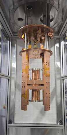
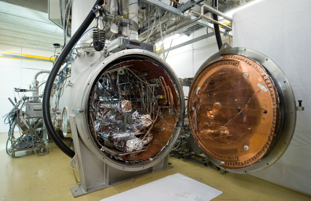
Integrate the Nb₃Sn-coated SRF cavity from Task 4.3 into a cryostat and test it under beam-relevant conditions, addressing two key challenges: a) replacing liquid helium cooling with conduction cooling for a simplified setup, and b) using off axis couplers while maintaining adaptable input coupling.
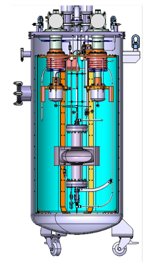
The bare cavity will be tested at HZB’s HoBiCaT facility, where thermal contact methods will be optimised and the helium line will be replaced by a cryocooler. HZB will design a beam-compatible TESLA-type cavity with added ports for a power coupler and pickup antenna, with RI supporting high-power coupler integration. In parallel, CEA will design a cryostat using a closed-loop liquid helium system for vertical and horizontal testing of 1.3 GHz cavities at 4.2 K. This system will feature a 3D-printed Cu-based double-wall structure embedded in the Nb₃Sn-coated cavities. The two approaches will assess the impact of microphonics from cryocoolers and helium boiling, respectively, on cavity RF performance and develop mitigation strategies.
Task 4.3: 1.3 GHz cavity production and coating
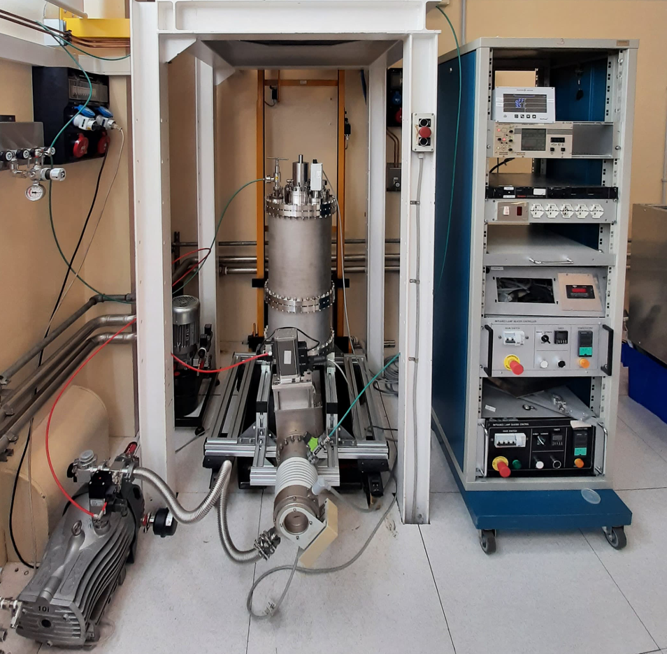
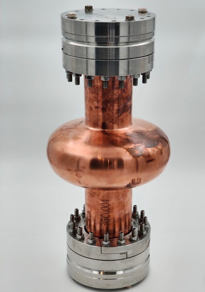
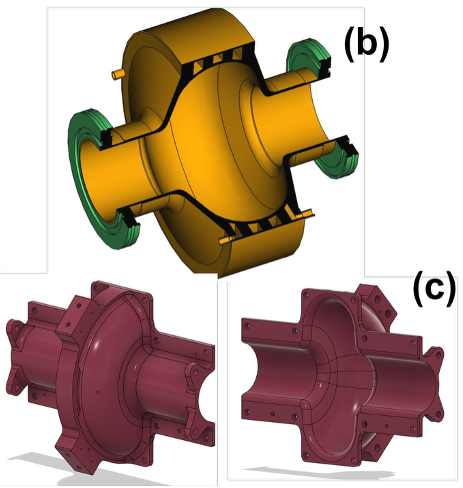
Deliver single cell 1.3 GHz copper cavities, with integrated power coupler and pick up ports and coated with Nb₃Sn superconducting thin films, for use in Task 4.2. Cavities will be produced through seamless fabrication at INFN and equator Electron Beam welding at Zanon and RI. Additive Manufacturing will also be explored by CEA and INFN. Cavity polishing will be performed at INFN, and Zanon. CEA and UKRI will set up surface preparation facilities leveraging partner experience.
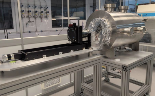
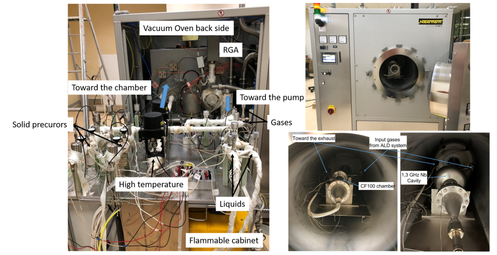
Superconducting TF coating will be carried out at CEA, INFN, and UKRI using different setups to reduce failure risk. Zanon will build a new industrial coating facility based on experience gained in I.FAST, with systems optimised to also coat the power coupler and pickup ports doors. In parallel, TF deposition on longitudinally split cavity geometry will be explored by UKRI, with the support of Lancaster University. The baseline coating protocol will follow I.FAST developments, while CEA will assess the possibility of including interlayers via Atomic Layer Deposition (ALD) based on the results of IEE.
Few example of 1.3 GHz cavities to be coated
Task 4.4: Superconducting thin film development
The goal of this task is to develop cylindrical sputtering targets for Task 4.3, new high temperature stable substrates for Nb3Sn deposition and continue superconducting thin films R&D on new superconducting alloys using state of art characterization techniques and post thermal treatments.